FIELD: thin films technology and multi-layer nano-structures.
SUBSTANCE: "metallic film - semiconductor or insulating substrate" structure is exposed to microwave radiation using a wave guide system. In front of the structure there is a dielectric plate with thickness L, and dielectric coefficient εd, for which, in the chosen frequency range on one of the frequencies ω1, the condition 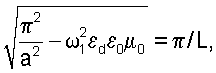 holds, and on another frequency ω2, the
 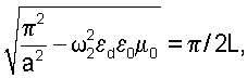 condition holds, where a is the typical size of the cross-section of the wave guide system, ω=2πf is the angular frequency of the radiation, and ε0 and μ0 are the dielectric and magnetic permittivity in a vacuum, respectively. Relative dielectric permittivity of the chosen dielectric plate should be more than 2. Electro-conductivity or thickness of the metallic film is determined from the frequency response of the reflection coefficient of the structure.
EFFECT: broader range of the measured thickness and class of the analysed materials and increased sensitivity.
2 cl, 6 dwg
| Title | Year | Author | Number |
|---|---|---|---|
| ELECTROPHYSICAL MEASUREMENT METHOD FOR NANOSCALE METAL FILM ON SEMICONDUCTOR OR DIELECTRIC SUBSTRATE STRUCTURE | 2007 |
|
RU2349904C1 |
| METHOD OF MEASURING PARAMETERS OF SEMICONDUCTOR STRUCTURES | 2015 |
|
RU2622600C2 |
| METHOD TO DETERMINE ELECTROCONDUCTIVITY AND THICKNESS OF SEMICONDUCTOR PLATES OR NANOMETER SEMICONDUCTOR LAYERS IN STRUCTURES "SEMICONDUCTOR LAYER - SEMICONDUCTOR SUBSTRATE" | 2012 |
|
RU2517200C2 |
| DEVICE FOR MEASURING RELATIVE PERMITTIVITY AND LOSS-ANGLE TANGENT OF LIQUID | 2010 |
|
RU2419099C1 |
| DEVICE FOR DETERMINATION OF PARAMETERS OF METAL-DIELECTRIC STRUCTURES | 2013 |
|
RU2534728C1 |
| METHOD FOR DETERMINATION OF CONDUCTIVITY AND THICKNESS OF SEMICONDUCTOR LAYERS | 2010 |
|
RU2439541C1 |
| BROADBAND WAVEGUIDE TERMINATION | 2008 |
|
RU2360336C1 |
| METHOD TO DETERMINE ELECTROCONDUCTIVITY AND ENERGY OF ACTIVATION OF ADMIXTURE CENTRES OF SEMICONDUCTOR LAYERS | 2012 |
|
RU2516238C2 |
| TRANSPARENT STRUCTURE FOR MICROWAVE SIGNAL MODULATION | 2023 |
|
RU2802548C1 |
| WAVEGUIDE MATCHED LOAD | 2015 |
|
RU2601612C1 |

