FIELD: physics.
SUBSTANCE: in the method of selecting CMOS/SOI transistor structures which are resistant to the effect of full absorbed dose of ionising radiation, for each process solution, an additional pair of n- and p-channel transistor channels made from the same technology is formed on the chip along with the main LSI circuit; for limited sampling, LSI specimens are removed discretely with a step of about 100 krad(Si) in the TID range from zero to the level of requirements for resistance of the LSI to the effect of maximum TID plus 20% of the relationship ID=f(VGs); data are obtained therefrom on change in shift of threshold voltage ΔVTH from the TID value through a dose of not less than about 1000 rad(Si)·s-1 taking into account manufacturing tolerance and possible boundaries of variation of the relationship VTH(TID); lower  and upper
  allowable boundaries of relationships VTH(TID) of transistors of both conductivity types are approximated; the dispersion of measured values
 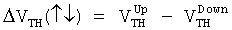 is determined for each fixed TID value; the value ΔVTH(↑↓) without exposure is determined for the minimum on the curve
  for an n-channel transistor and for the virtually achieved maximum level of exposure; ΔVth(↑↓) is determined for the same conditions for all possible combinations of differences "VTh(TID)-Up" and "Vth(TID)-Down" of n-MOS and p-MOS transistors, ΔVth(↑↓) is determined for three fixed LSI TID values; the LSI are ranked on four gradations of the observed values of ΔVth(↑↓): "high" ("1") - maximum change; "significant" ("2") - strong change; "average" ("3") - moderate changes; "low" ("4") - weak changes, which on the average value are sorted as "1"%:"2"%:"3"%:"4"%, where the "low" gradation is taken as 100%; ΔVth(↑↓) is measured for non-exposed industrial LSI specimens and the results of ranking exposed specimens are used to determine the possibility of using in exposure conditions those specimens for which the gradation of change in the value of ΔVth(↑↓) corresponds to categories "4" and "3".
EFFECT: possibility of selecting industrial LSI which are resistant to TID effects without conducting an exposure experiment to measure radiation drift of threshold voltage ΔVth.
7 dwg
| Title | Year | Author | Number |
|---|---|---|---|
| METHOD TO DETERMINE COEFFICIENT OF RELATIVE EFFICIENCY AND EQUIVALENT DOSE OF SOURCE OF X-RAY RADIATION | 2011 |
|
RU2480861C1 |
| METHOD TO TEST SEMICONDUCTOR CMOS/SOI OF LSI TECHNOLOGY FOR RESISTANCE TO EFFECTS OF SINGLE FAILURES FROM IMPACT OF HEAVY CHARGED PARTICLES OF SPACE | 2011 |
|
RU2495446C2 |
| METHOD FOR EVALUATING RESISTANCE OF DIGITAL ELECTRONIC EQUIPMENT TO IONISING RADIATION (VERSIONS) | 2014 |
|
RU2578053C1 |
| METHOD FOR COULOMETRIC MEASUREMENT OF ELECTRIC PARAMETERS FOR n-MOS TRANSISTORS NANOSTRUCTURES IN TECHNOLOGIES OF COMPLEMENTARY MOS LOGIC (CMOS)/SILICONE-ON- INSULATOR | 2010 |
|
RU2439745C1 |
| DEVICE FOR COULOMETRIC MEASUREMENT OF ELECTROPHYSICAL PARAMETERS OF n-MOS TRANSISTOR NANOSTRUCTURES IN CMOS/SOI TECHNOLOGIES | 2011 |
|
RU2456627C1 |
| CMOS SOI INTEGRAL CIRCUIT WITH HIGH RADIATION RESISTANCE (VERSIONS) | 2015 |
|
RU2601251C1 |
| MOS STRUCTURE MANUFACTURING TECHNIQUE | 1992 |
|
RU2012091C1 |
| METHOD FOR MANUFACTURING HIGH-TEMPERATURE CMOS SOI INTEGRATED CIRCUITS | 2016 |
|
RU2643938C1 |
| PROCESS OF MANUFACTURE OF MIS LARGE-SCALE INTEGRATED CIRCUITS | 1990 |
|
SU1762688A1 |
| CMOS IC OF HIGHER RADIATION RESISTANCE | 2013 |
|
RU2545325C1 |

