FIELD: manufacture of micromechanical and microelectronic sandwich-structure devices on substrate. SUBSTANCE: method for microprofiling SiC-AlN material includes plasma-chemical etching process with coating mask applied to SiC film areas followed by removal of AlN layer areas to open movable components of target product. All operations are made in quasi-enclosed chamber of reactive ion-plasma etching installation under high-frequency magnetron discharge at specific power of 1.4±4 W/sq. cm; masking material used for the purpose is aluminum; SiC film areas are etched at a pressure of 0.4±0,2 Pa in plasma of gas mixture SF6/O2, containing 15±5 volume percent of O2; AlN layer is removed at a pressure of 0.5±9.1 Pa in plasma of gas mixture C2Cl3F3/O2 containing 5±2 volume percent of O2. Ratio of pressure within chamber to specific power of high-frequency discharge should be best controlled by means of servo system using proportion 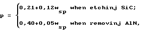 where p is pressure within quasi-enclosed chamber, Pa; wsp is specific power of magnetron discharge, W/sq. cm. Final operation for producing structure on silicon substrate involves deep local etching of the latter in plasma of SF6/O2, gas mixture containing 12±8 volume percent of O2, at a pressure of 0.6±0.2 Pa. EFFECT: facilitated procedure due to using single processing installation and unified technology. 3 cl, 2 dwg, 3 tbl
| Title | Year | Author | Number |
|---|---|---|---|
| PROCESS OF MANUFACTURE OF MICROMECHANICAL INSTRUMENTS | 1998 |
|
RU2137249C1 |
| MICROMECHANICAL GAGE AND ITS MANUFACTURING PROCESS | 1999 |
|
RU2170993C2 |
| HIGH-TEMPERATURE SEMICONDUCTOR DEVICE AND PROCESS OF ITS MANUFACTURE | 2000 |
|
RU2166221C1 |
| METHOD FOR CONTROLLING GROWTH OF EPITAXIAL SEMICONDUCTOR STRUCTURE | 1998 |
|
RU2132583C1 |
| METHOD OF CONTROL OVER PROCESS OF WINNING OF SEMICONDUCTOR STRUCTURE | 2001 |
|
RU2188477C1 |
| SILICON-ON-INSULATOR STRUCTURE FOR MANUFACTURING SEMICONDUCTOR DEVICES AND ITS PRODUCTION METHOD | 2002 |
|
RU2193255C1 |
| METHOD OF GROWING LAYER OF HARD CARBON | 2001 |
|
RU2202513C1 |
| METHOD FOR PLASMA ETCHING OF INSULATING LAYERS | 2001 |
|
RU2211505C2 |
| PROCESS OF PLASMA-CHEMICAL PICKLING OF SILICON-CARRYING MATERIALS | 1997 |
|
RU2141701C1 |
| METHOD FOR PRODUCING SUBMICRON AND NANOMETRIC STRUCTURE | 2005 |
|
RU2300158C1 |

