FIELD: measurement equipment.
SUBSTANCE: in the method to control defect structure of epitaxial silicon layers on dielectric substrates, including preparation of the sample surface, exposure to radiation with wave length λ=380÷630 nm to a sample, rotating around the vertical axis and moving in the horizontal direction relative to the falling radiation, registration of amplitudes of the recorded signal, calculation of relative defect structure of the epitaxial layer Ndef and comparison of the calculated value Ndef with the available value Ndef (ref) of the comparison reference, the sample is exposed to pulses with duration of τ1=50÷100 mcs and porosity τ2=250÷500 mcs, the recorded signal is the amplitude Uout of the induced photo-EMF in the epitaxial layer of silicon, and relative defect structure of the epitaxial layer is calculated based on the ratio: 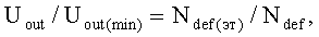
EFFECT: high efficiency of measurements and valid assessment of concentration of defects in volume of an epitaxial silicon layer at the border of silicon-sapphire.
1 dwg
| Title | Year | Author | Number |
|---|---|---|---|
| METHOD FOR FLAW INSPECTION OF SILICON FILMS ON INSULATING SUBSTRATES | 2000 |
|
RU2185684C2 |
| METHOD OF PRODUCING DIODE OPTOELECTRONIC PAIRS RESISTANT TO GAMMA-NEUTRON RADIATION | 2020 |
|
RU2739863C1 |
| PHOTODETECTOR (VERSIONS) AND PRODUCTION METHOD THEREOF | 2015 |
|
RU2611552C2 |
| METHOD TO MODIFY SURFACES OF METALS OR HETEROGENEOUS STRUCTURES OF SEMICONDUCTORS | 2011 |
|
RU2502153C2 |
| METHOD FOR DETERMINING THE EFFECTIVE LIFETIME OF NONEQUILIBRIUM CHARGE CARRIERS IN P(N) LAYERS OF LOCAL SECTIONS OF N-P(N)-P TYPE SILICON SOLAR CELLS | 2022 |
|
RU2789711C1 |
| METHOD FOR PRODUCING HETEROEPITAXIAL SILICON LAYER ON DIELECTRIC | 2016 |
|
RU2646070C1 |
| METHOD OF CONTACT-FREE DETERMINING OF CHARACTERISTICS OF SILICON PLATES PROVIDED WITH INTERNAL GETTER | 1991 |
|
RU2009575C1 |
| METHOD FOR CONTROL OF DEFECTIVENESS AND RESILIENT DEFORMATION IN SEMICONDUCTOR HETEROSTRUCTURES LAYERS | 2010 |
|
RU2436076C1 |
| FLAW INSPECTION METHOD FOR SILICON-ON-INSULATOR FILMS | 2004 |
|
RU2256256C1 |
| METHOD FOR TREATMENT OF SILICON-ON-SAPPHIRE STRUCTURES | 2000 |
|
RU2185685C2 |

