FIELD: semiconductor industry.
SUBSTANCE: invention relates to the technology of manufacturing semiconductor devices. In the method for obtaining an epitaxial calcium silicide film, CaF2 is first deposited on a substrate with a silicon layer on its working surface, a CaF2 layer is formed from 4 to 10 nm or from 20 to 40 nm. Then, at the same time, ionizing radiation particles are irradiated with energy that provides excitation, decomposition and formation of atomic Ca in relation to CaF2, and high-temperature treatment is carried out. The treatment is carried out by maintaining the heated state of the substrate to the temperature and the passage of time, providing, in relation to the irradiated sections of the CaF2 layer, a layer of calcium silicide CaSi2 of a characteristic 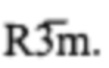 spatial group is obtained. In another variant of the method, CaF2 is simultaneously deposited on the silicon layer, irradiated with ionizing radiation particles, and high-temperature treatment is carried out over time, providing for the irradiated deposition sites of CaF2 to obtain a layer of calcium silicide CaSi2 of a characteristic spatial group , the deposition of CaF2 is carried out with respect to the amount of calcium difluoride, which is equivalent in terms of the formed thickness of the layer of CaF2 from 4 to 10 nm or from 20 to 100 nm during the time providing for the irradiated deposition sites of CaF2 to obtain a layer of calcium silicide.
EFFECT: obtaining a strictly specified, single, polytype of the formed CaSi2 film with the realization of obtaining both 6R and 3R polytype characteristic of the spatial group .
8 cl, 5 dwg
| Title | Year | Author | Number |
|---|---|---|---|
| METHOD FOR PRODUCING STRUCTURES WITH BURIED METAL LAYER | 1992 |
|
RU2045795C1 |
| PROCESS OF MANUFACTURE OF MESOTAXIAL LAYERS OF COBALT DISILICIDE IN SILICON | 1990 |
|
SU1795821A1 |
| METHOD TO MODIFY SURFACES OF METALS OR HETEROGENEOUS STRUCTURES OF SEMICONDUCTORS | 2011 |
|
RU2502153C2 |
| METHOD OF OBTAINING STRUCTURED SEMICONDUCTOR SURFACE | 2012 |
|
RU2519865C1 |
| LATERAL BIPOLAR TRANSISTOR BASED ON “SILICON ON INSULATOR” STRUCTURES AND THE METHOD FOR ITS MANUFACTURE | 2021 |
|
RU2767597C1 |
| METHOD FOR DETERMINING THE ENERGY EQUIVALENT OF THE THICKNESS OF THE DEAD LAYER OF THE DETECTOR | 2020 |
|
RU2756359C1 |
| METHOD OF FORMING EPITAXIAL COPPER NANOSTRUCTURES ON SURFACE OF SEMICONDUCTOR SUBSTRATES | 2013 |
|
RU2522844C1 |
| METHOD FOR GROWING SEMICONDUCTOR FILM | 2023 |
|
RU2814063C1 |
| METHOD OF FORMING ORDERED STRUCTURES ON SURFACE OF SEMICONDUCTOR SUBSTRATES | 2015 |
|
RU2593633C1 |
| METHOD OF MODIFYING NANOSTRUCTURES OF ELECTRONIC ENGINEERING MATERIALS WITH GAS CLUSTER IONS | 2016 |
|
RU2688865C2 |

